3DAP-TIME: 3D Acoustic Processing To Inspect Manufactured Electronics
Modern electronic systems are becoming ever smaller and more difficult to test and inspect. The recent advances towards 3D chip technology with multi-die and many layered devices demands new methods for inspection and reliability testing. Roadmaps such as ITRS have indicated that new methods for metrology to test manufactured devices are urgently required. For the non-destructive inspection of hidden layers and connections of the thin layered devices now being produced needs a new breakthrough in inspection methods.
In this TTP, the focus is twofold, firstly to build an acoustic processing system to extract previously hidden details in 3D and secondly to control the acquisition and image processing via an intuitive users interface. The benefits of the work completed are:
- To differentiate and locate in 3D for the first time where manufacturing faults or failures have occurred inside electronic devices and systems. Present acoustic inspections systems are 2D and can’t accurately detect at which layer faults occur in the limit as the acoustic signals start to overlap due to the limited axial resolution.
- An intuitive user interface that has enabled selection and operation of a suite of in-house processing algorithms to enable rapid failure analysis of manufactured electronics.
Sonoscan is a pioneer in the design of acoustic microscopes for micro-imaging in the electronics industry. As such they are always looking for new opportunities to improve their products. They have strong market penetration and most failure analysis laboratories will have one of their acoustic micro-imaging systems. By attempting to gain resolution through advanced signal processing, new results with thin layered devices will be possible without having to change existing sensors. As such the processing can be retrofitted to existing instruments when compatible with the existing user interface. This will enable superior testing and reliability measurement than is presently available.
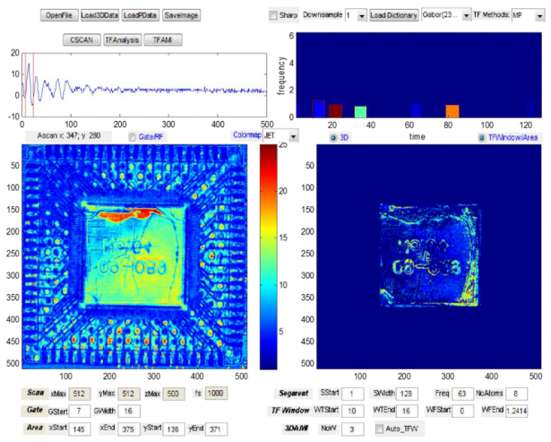
Figure 1 Example of user interface showing input, filter and output windows with control buttons
The acoustic signal processing systems is controlled by a graphical user interface designed as shown in Figure 1. The user windows are:
- Top Left, Acoustic A-scan signal acquisition and gate control
- Bottom Left, C-scan or 2D layer as selected by control buttons
- Top Right, time-frequency filter selection and control
- Bottom Right, Layer(s) output and control
The introduction of filtering in the time-frequency domain together with some sparse-signal processing and selected signal dictionaries enabled the unravelling of overlapped acoustic signals and discrimination of individual fault planes.
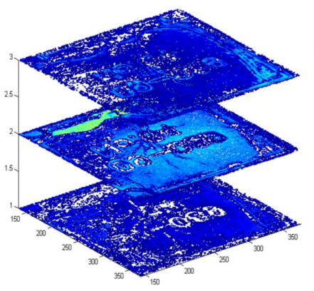
Figure 2 Separation of Individual Layers for accurate location of any delamination or fault
For standard acoustic micro-imaging systems the delamination shown in Figure 2 would not be able to be pinpointed in electronic designs with very thin layers. The acoustic processing previously developed, and now implemented in this TTP supports wider applications for testing modern devices. More precise location of manufacturing or reliability faults is now possible, to help better identify at which vertical plane they exist.
In the TTP, advice from Sonoscan has informed the design and processing of the acoustic signals. Some algorithms were parallelized and this afforded significant speed-up on a standard PC which was the target processor. The design of the user interface is fine as a prototype, was stable and works very well. Integration within the Sonoscan instrument environment is still required with an even simpler user interface before the company thinks it will be acceptable to users. A user manual developed to help operate the acoustic signal processing system has been delivered to Sonoscan, with hands-on training of the system performed at the company’s site. In conclusion, the system has been successfully delivered to Sonoscan, and future work will continue to speed-up the algorithms and better integrate the user interface. When this has been done it can start to be retrofitted to instruments in the field and on new instruments, giving unprecedented accuracy to acoustic measurement of manufactured electronics.